

Total support from surveys and estimates to sorting and collection and transportation.
Grants are provided for the treatment and analysis of PCB waste.
〜We provide periodic free seminars on grant procedures.〜
Tokyo Trace PCB Waste Disposal Support Project
Grantee
⓵ Individuals / ⓶ Small and medium sized enterprise groups / ⓷Building management union corporations
⓸SME’s / ⓹Entities other than corporations (Education institutes, medical institutes, foundations, religious organizations, social welfare organizations, nursery schools, health insurance groups, etc.)
Analysis
Analyze electrical equipment held in Tokyo.
Processing
We process insulating oil, containers, and electrical equipment that have been verified in Tokyo and contain trace PCBs.
The deadline for processing PCB waste is approaching.
Early Treatment of Waste from PCB Ballasts and One Stop Service
We can propose a series of services related to the treatment of high concentration PCB contaminated electrical devices. By contracting work, transportation, and processing at one time, we will not only execute the whole process smoothly but also simplify the documentation procedures while reducing the burden on you. In addition, managing separately reduces the risk of problems such as problems caused by lack of communication. From the time of planning this burdensome work, we will offer proposals according to each customer's circumstances. We will pursue customer service from transportation and processing of PCB waste to recycling and hold ourselves to very high expectations.
Did you know?
There is a legal penalty if you do not dispose within the time limit.For PCB waste, the PCB Special Measures Act was established during June 2001 requiring high concentration PCB waste stored by business operators to be properly disposed of by March 31, 2023. For buildings and structures built prior to March 1977, a survey of PCB usage and storage will be required.
The Processing deadline for high concentration PCB waste is approaching.
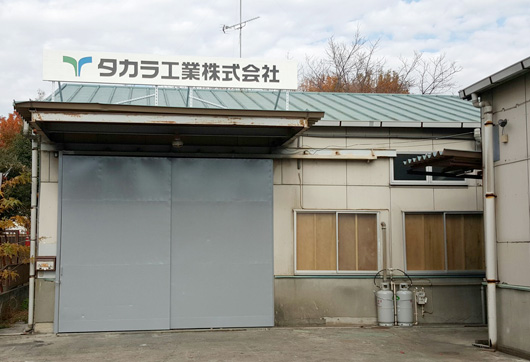
Our company owns a dedicated storage warehouse for PCBs, and we are a company that can provide total support from surveys and estimates, to sorting and collection and transportation, without the need of another hand. First, please contact us so we can flexibly respond to your situation.
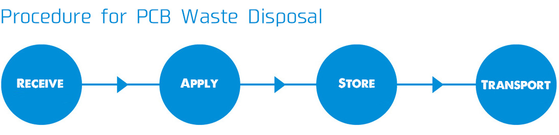
PCB waste disposal procedures
Early treatment of waste from PCB Ballasts and One Stop Service
1.Elimination of non-PCB ballasts by salvage / sorting operations
2.Application / import package form a survey table
3.Storage / dedicated storage facility with transport
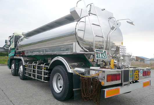
4.Transporting / transportation to Hokkaido JESCO
We have our own PCB storage warehouse,
We will provide one-stop support without hassle.
Takara Industries Service Features
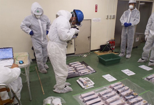
1. Sorting and preparing a Package Registration
In order to properly process PCB contained ballasts stored by customers, we sort out and separate the PCB contained ballasts and prepare loading instructions for disposal at the Japan Environmental Storage and Safety Corporation (JESCO).
2. Safe, proper work and a storage warehouse exclusively for PCBs
Sorting and separating are handled by experienced staff while carrying out safe and appropriate work in accordance with the guidance manual of the Ministry of the Environment. In addition, we have prepared a dedicated storage warehouse for PCB waste. This makes it possible to pick up PCB waste that could not be carried out from customers' warehouse for many years.
3. One stop service
The process begins with a survey and approximate estimate, followed by steps involving picking up waste from PCB ballasts, sorting and package preparation, storing, collection and transportation, and with delivery to the final disposal site at Hokkaido JESCO.
About PCB waste
PCBs (polychlorinated biphenyl) are a colorless and transparent oily substance with various excellent properties such as flame-retardant, chemical and thermal stability, and high insulation. In the past, it was used for insulation oil for transformers and capacitors, as a heat transfer medium (catalyst oil), lubricating oil, pressure-sensitive copying paper, etc. However, it has been found that if it enters the human body, it causes severe chronic diseases thus production was discontinued during 1972. PCBs do not degrade easily in the environment because of their unstable properties and when released into the environment they diffuse toxicity. In addition, it has been reported to cause global-scale contamination (accumulation in human bodies, seals, whales, etc.) because it has the property of being easily concentrated in the body of an organism via the food chain. PCB waste must first be properly stored to prevent the spread by leakage. It is necessary to disassemble and dispose of it properly as soon as possible.
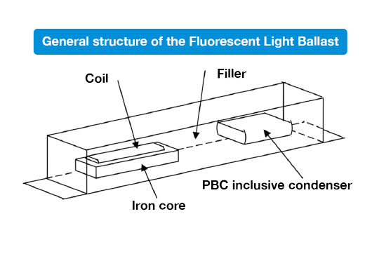
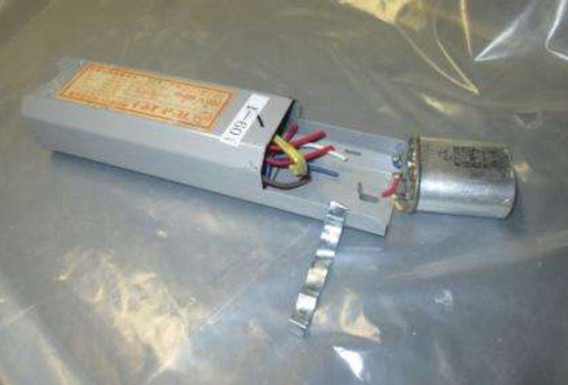
1.Fixated device
Ballasts consist of coils, a core, capacitors, etc., and in many cases, the space in the container is filled with asphalt or resin to fixate the equipment.
2.Concern over environmental impact
If the ballast containing high concentrations of PCB became waste, it was reported that the contamination with PCB was reported in the area other than the capacitor, and there is concern about the environmental impact. We must store them after classification processing and dispose of them by March 31, 2023.
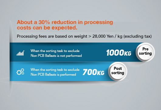
Realization of cost reduction
Please let Takara Industries reduce the weight of PCB-containing ballasts.
Precision sorting and analysis has become possible through working in our special warehouse, while also the ability to reduce weight of the PCB-containing Ballasts. At the same time, final disposal fees for JESCO are expected to be significantly reduced.
When thinking about disposing PCBs, think Takara Industries
If you want to outsource the disposal of PCBs in the Kanto suburbs, please use Takara Industries in Minato-ku, Tokyo. Takara Industries has a dedicated storage facility for PCB waste and offers a full package of services related to PCB waste disposal. Please be assured we will do our best to help you reduce your PCB waste disposal burden by undertaking the entire process in a single operation.
The final disposal costs can be reduced to ensure accurate sorting within the dedicated storage warehouse and to achieve thorough weight reduction. We also provide support for grant applications, so please feel free to contact us if you want to use grants and subsidies for PCB waste disposal. We are flexible and will respond to your situation and circumstances.
Consultation on disposal of PCBs with Takara Industries
| Company Name | Takara Industries Co., Ltd. |
|---|---|
| Address | 2-2-3 Nishi Shinbashi Building 6th Floor, Nishi Shinbashi Minato-ku, Tokyo, 105-0003 |
| TEL | 03-6206-6481 |
| FAX | 03-6206-6482 |
| Factory Address | 4-20-1 Ukima, Kita-ku, Tokyo 115-0051 |
| Factory TEL | 03-5948-7901 |
| Factory FAX | 03-5948-7902 |
| info@takarakogyo.jp | |
| Business Content | Collection, transportation, and processing of specially controlled industrial waste; Nondestructive inspection soil improvement; Resource recycling activities; Research on chemicals that make harmful substances harmless; Development and sales; Other |
| Business Hours | Weekdays:9:00 〜 17:30 |
| Banking Branch | Mizuho Bank Shinbashi Branch / Jonan Credit Union Shinbashi Branch |
| URL | http://takarakogyo.jp/ |